 Image 1 of 1
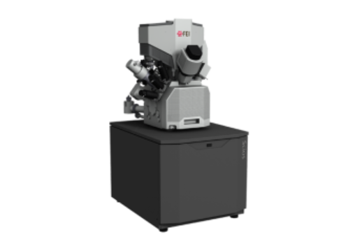
Our business provides specialized Focused Ion Beam (FIB) equipment and accessories to support advanced laboratories, research institutions, and engineering facilities. We supply high-quality tools and components to ensure reliable performance, system longevity, and precise results in applications such as semiconductor analysis, failure analysis, materials research, and microfabrication.
A dual-beam Focused Ion Beam (FIB) system is a high-precision instrument that combines two powerful imaging and processing technologies in one platform:
Focused Ion Beam (FIB): Uses a finely focused beam of ions to mill, cut, or modify materials at the micro- and nanoscale.
Scanning Electron Microscope (SEM): Provides high-resolution imaging of the sample’s surface.
By integrating both beams, dual-beam FIB devices allow researchers and engineers to simultaneously observe and modify materials with nanometer-level precision, making them essential in chip analysis, defect inspection, and advanced materials research.